SRAM_1024x32
Overview
This is a 1024 words by 32 bits commercial grade low power embedded Single Port Synchronous (flow through) SRAM in SKY130 technology. An active high read-write enable signal controls the read/write operation of the memory. When bit-enable is high and readwrite enable is low, data on the data input pin is written into the memory location addressed by the address present on the address pins. Reading the device is accomplished while read-write enable is high. Under these conditions, the contents of the location addressed by the information on address lines is present on the data output pin. In write cycle, data to be written is driven onto data output pin. If there is no read or write, while memory is enabled, data output pin will hold previous data.
Memory dimesions in SKY130 technology: 387.870 um x 303.315 um = 0.118 mm2
Installation
You can implement as many instances of the above macros in a single ChipCreate project for the same price.
Installation of the above macros is through IPM. To install IPM and the SRAM_1024x32 IP, follow these steps:
pip install cf-ipmipm install CF_SRAM_1024x32See the detailed information for the base macro here.
Memory Features
- Synchronous Read-Write
- Active High Bit Enables
- Single Read-Write Enable (Low = write, High = read)
- Write on a bit basis
- Separate pins for data input and data output
- Separate Power Supplies for core and periphery
- Body bias option
- Scan Chain Testmode
- Wafer Level Burn-In Testmode
- Option to switch off all wordlines while chip is enabled
- Option for Power Switch
- Clock Gating
Block Diagram
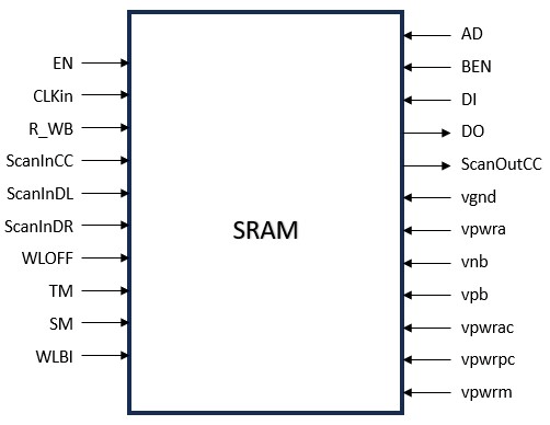
Pin Description
| NAME | TYPE | DIRECTION | DESCRIPTION |
|---|---|---|---|
| AD [9:0] | CMOS | IN | This input value selects the location to be read during a read cycle, and the location to be written during a write cycle. It is sampled on rising edge of clock. |
| R_WB | CMOS | IN | This is the read/write control and sampled on rising edge of clock. When R_WB is high, the memory is in a read cycle mode. When R_WB is low, the memory is in write cycle mode. |
| CLKin | CMOS | IN | Clock synchronizes the operations of the memory. All inputs are sampled on rising edge of clock. |
| BEN [31:0] | CMOS | IN | Each bit of the BEN bus selects one bit of the DI bus. When one or more BEN inputs are high (active), and R_WB is low (write enabled) then the selected bits will be written into the memory. |
| DI [31:0] | CMOS | IN | This data is written into the memory location selected by addr input during the write cycle. It is ignored during a read cycle. |
| EN | CMOS | IN | EN (Chip Enable) is high (and TM low), read and write operation is performed. |
| TM | CMOS | IN | When TM (Testmode)is high, memory is in testmode and normal memory operation is disabled. Inputs are tied to outputs through scan chain logic. |
| SM | CMOS | IN | When SM (Scan chain control) is high, output of a input register is passed to next register. When low, input register receives input from input pin. |
| WLBI | CMOS | IN | Wafer Level Burn-In Test mode control: When high, all wordlines are ON. |
| WLOFF | CMOS | IN | Normal operation when low. All wordlines are clamped to vnb when high. |
| ScanInCC | CMOS | IN | Input to Address and Control scan chain. |
| ScanInDL | CMOS | IN | Input to Data scan chain (left side of the macro). |
| ScanInDR | CMOS | IN | Input to Data scan chain (right side of the macro). |
| DO [31:0] | CMOS | OUT | Data from the memory location selected by address is driven onto DO during a read cycle. In a write cycle, data to be written is driven onto DO. If there is no read or write, while memory is enabled, DO will hold previous data. |
| ScanOutCC | CMOS | OUT | Output of Scan Chain of address and control pins. Note - DO is output of scan chain of data input pins. |
Without the Power Switch feature enabled (default recommended mode)
| NAME | TYPE | DIRECTION | DESCRIPTION |
|---|---|---|---|
| vpwrm | Supply | IN | Connect vpwrm to core power supply vpwra |
| vpwra | Supply | IN | Nominal 1.8 power supply to memory array |
| vpwrp | Supply | IN | Nominal 1.8 power supply to periphery |
| vpwrac | Supply | IN | Connect vpwrac to core power supply vpwra |
| vpwrpc | Supply | IN | Connect vpwrpc to core power supply vpwra |
| vgnd | Supply | IN | Nominal 0 V power supply (ground). |
| vpb | Bias Voltage | IN | Nwell connection, tie to the maximum power supply (can be vpwra or vpwrp) |
| vnb | Bias Voltage | IN | Pwell connection, nominally equal to vgnd |
With the Power Switch feature enabled
| NAME | TYPE | DIRECTION | DESCRIPTION |
|---|---|---|---|
| vpwrm | Supply | IN | Nominal 1.8 main power supply |
| vpwra | Supply | IN | power supply to memory array (internal node) |
| vpwrp | Supply | IN | power supply to periphery (internal node) |
| vpwrac | Supply | IN | Control signal to turn on the power supply to periphery (active LOW, CMOS) |
| vpwrpc | Supply | IN | Control signal to turn on the power supply to core (active LOW, CMOS) |
| vgnd | Supply | IN | Nominal 0 V power supply |
| vpb | Bias Voltage | IN | Nwell connection, tie to the maximum power supply (can be vpwrm) |
| vnb | Bias Voltage | IN | Pwell connection, nominally equal to vgnd |
Specifications
DC Specifications
Conditions
- Process Condition : Typical
- Junction Temperature : 25.000 deg C
- Operating Voltage : 1.800 V
- Operating Frequency : 100 MHz
Power Dissipation When R_WB=HIGH
- READ Active = 77.566 pJ
- READ Active = 8.618 mA
- READ Peak = 80.613 mA
Power Dissipation When R_WB=LOW
- WRITE Active = 69.948 pJ
- WRITE Active = 7.772 mA
- WRITE Peak = 79.072 mA
Power Dissipation When EN=LOW, All Other Inputs Switching
- Standby = 0.174 pJ
- Standby = 0.019 mA
- Standby Peak = 0.470 mA
Power Dissipation When TM=HIGH, Clock Switching
- Test Mode = 9.603 pJ
- Test Mode = 1.067 mA
- Test Peak = 33.687 mA
Leakage: Power switches ON, Disabled (EN=LOW)
- Power = 41611.200 pW
- Current = 23.120 nA
Leakage - One or More Power switches OFF (VPWRPC=HIGH or VPWRAC=HIGH)
- Power = 1420.430 pW
- Current = 0.790 nA
AC Specifications
Conditions
- Process Condition : Typical
- Junction Temperature : 25.000 deg C
- Operating Voltage : 1.800 V
- Operating Frequency : 100 MHz
| DESCRIPTION | SYMBOL | MIN SPEC (ns) | MAX SPEC (ns) | ACTUAL (ns) |
|---|---|---|---|---|
| Cycle Time | Tcyc | 8.000 | ||
| Clock High Time | Tchi | 4.000 | ||
| Clock Low Time | Tclo | 4.000 | ||
| Clock to data-out (Read Cycle) | Trd | 0.500 | 4.74 | Rise: 2.441 Fall: 2.455 |
| Clock to data-out (Write Cycle) | Twr | 0.500 | 4.04 | Rise: 2.041 Fall: 2.055 |
| Setup time of addr/ctrl to clk | Tsad | 0.500 | Rise: 0.527 Fall: 0.617 | |
| Setup time of EN to clock | Tsen | 1.300 | 1.376 | |
| Hold time of addr/ctrl from clk | Thad | 0.700 | Rise: 0.326 Fall: 0.325 | |
| Setup time of Data to clk | Tsdi | 0.700 | 0.832 | |
| Hold time of data from clk | Thdi | 1.000 | 0.486 | |
| Setup time of BEN to clk | Tsben | 0.700 | 0.821 | |
| Hold time of BEN from clk | Thben | 1.000 | 0.504 |
Test Mode Parameters
| DESCRIPTION | SYMBOL | MIN SPEC (ns) | MAX SPEC (ns) | ACTUAL (ns) |
|---|---|---|---|---|
| Clock to data-out (Test Mode) | Tcotm | 0.150 | 3.570 | Rise: 1.621 Fall: 1.635 |
| Clock to ScanOutC (Test Mode) | Tcotm | 0.150 | 3.570 | Rise: 1.748 Fall: 1.735 |
| Setup time of Add & Control to clk (Test Mode) | Tsctl_tm | 0.800 | Rise: 0.849 Fall: 0.878 | |
| Hold time of Add & Control to clk (Test Mode) | Thctl_tm | 0.550 | Rise: 0.574 Fall: 0.568 | |
| Setup time of TM, SM to clk | Tstm | 6.500 | 6.500 | |
| Hold time of TM, SM from clk | Thtm | 1.000 | 1.000 |
Timing Diagram
